
The field-effect transistor (FET) is a transistor that uses an electric field to control the electrical behaviour of the device. FETs are also known as unipolar transistors since they involve single-carrier-type operation. Many different implementations of field effect transistors exist. Field effect transistors generally display very high input impedance at low frequencies. The conductivity between the drain and source terminals is controlled by an electric field in the device, which is generated by the voltage difference between the body and the gate of the device.
Classification :
A field effect transistor is abbreviated as a FET. It is a semiconductor device in which the current is controlled by an electric field. A FET is an example of a unipolar device it works only depending on the majority carriers. FETs are voltage controlled devices, in contrast to bipolar transistor which are current controlled.
FETs are basically classified in to two categories.
- Junction field effect transistors ( JFET simply called as FET )
- Metal Oxide semiconductor Field Effect Transistor ( MOSFET )
The MOSFETs are also called as insulated gate field effect transistor (IG GET). MOSFETs are again two types.
(a) Enhancement mode MOSFET
(b) Depletion mode MOSFET
Principle and Working of JFET
Principle of JEFT
The two pn junctions at the sides form two depletion layers.The current conduction by charge carriers (i.e. electrons) is through the channel between the two depletion layers and out of the drain.The width and hence resistance of this channel can be controlled by changing the input voltage VGS.The greater the reverse voltage VGS, the wider will be the depletion layer and narrower will be the conducting channel.The narrower channel means greater resistance and hence source to drain current decreases.Reverse will happen when VGS decreases.Thus JFET operates on the principle that width and hence resistance of the conducting channel can be varied by changing the reverse voltage VGS.
In other word, the magnitude of drain current ID can be changed by altering VGS.
Working of JEFT
Case-i:
When a voltage VDS is applied between drain and source terminals and voltage on the gate is zero as shown in fig.3(i), the two pn junctions at the sides of the bar establish depletion layers.
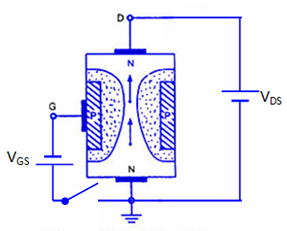
The electrons will flow from source to drain through a channel between the depletion layers.
The size of the depletion layers determines the width of the channel and hence current conduction through the bar.
Case-ii:
When a reverse voltage VGS is applied between gate and source terminals, as shown in fig.3(ii), the width of depletion layer is increased.
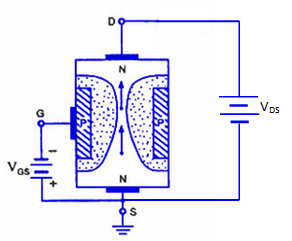
This reduces the width of conducting channel, thereby increasing the resistance of n-type bar.
Consequently, the current from source to drain is decreased.
On the other hand, when the reverse bias on the gate is decreased, the width of the depletion layer also decreases.
This increases the width of the conducting channel and hence source to drain current.
A p-channel JFET operates in the same manner as an n-channel JFET except that channel current carriers will be the holes instead of electrons and polarities of VGS and VDS are reversed.
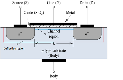
Working Principle of MOSFET:
The aim of the MOSTFET is to be able to control the voltage and current flow between the source and drain. It works almost as a switch. The working of MOSFET depends upon the MOS capacitor. The MOS capacitor is the main part of MOSFET. The semiconductor surface at the below oxide layer which is located between source and drain terminal. It can be inverted from p-type to n-type by applying a positive or negative gate voltages respectively. When we apply the positive gate voltage the holes present under the oxide layer with a repulsive force and holes are pushed downward with the substrate. The deflection region populated by the bound negative charges which are associated with the acceptor atoms. The electrons reach channel is formed. The positive voltage also attracts electrons from the n+ source and drain regions into the channel. Now, if a voltage is applied between the drain and source, the current flows freely between the source and drain and the gate voltage controls the electrons in the channel. Instead of positive voltage if we apply negative voltage , a hole channel will be formed under the oxide layer.

You must be logged in to post a comment.