What is a Transistor?
A transistor is one kind of semiconductor device that can both conduct and insulates. A transistor can perform as a switch and also an amplifier. It alters audio waves into electronic waves & resistor, controlling the flow of current. These components have very long life, small size, can function on lower voltage materials for better safety and not required filament current. The first transistor was made-up with germanium. A transistor does the same function as a vacuum tube triode, but consuming semiconductor junctions instead of excited electrodes in a vacuum chamber.
NPN

NPN Transistor Working
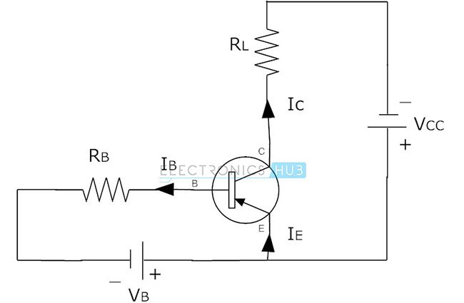
The working of NPN transistor is quite complex. In the above circuit connections we observed that the supply voltage VB is applied to the base terminal through the load RB. The collector terminal connected to the voltage VCC through the load RL. Here both the loads RB and RL can limit the current flow through the corresponding terminals. Here the base terminal and collector terminals always contain positive voltages with respect to emitter terminal.
If the base voltage is equal to the emitter voltage then the transistor is in OFF state. If the base voltage increases over emitter voltage then the transistor becomes more switched until it is in fully ON state. If the sufficient positive voltage is applied to the base terminal i.e. fully-ON state, then electrons flow generated and the current (IC) flows from emitter to the collector. Here the base terminal acts as input and the collector-emitter region acts as output.
To allow current flow between emitter and collector properly, it is necessary that the collector voltage must be positive and also greater than the emitter voltage of transistor. Some amount of voltage drop presented between base and emitter, such as 0.7V. So the base voltage must be greater than the voltage drop 0.7V otherwise the transistor will not operate. The equation for base current of a bipolar NPN transistor is given by,
IB = (VB-VBE)/RB
Where,
IB = Base current
VB = Base bias voltage
VBE = Input Base-emitter voltage = 0.7V
RB = Base resistance
The output collector current in common emitter NPN transistor can be calculated by applying Kirchhoff’s Voltage Law (KVL).
The equation for collector supply voltage is given as
VCC = ICRL + VCE ………… (1)
From the above equation the collector current for common emitter NPN transistor is given as
IC = (VCC-VCE)/RL
In a common emitter NPN transistor the relation between collector current and emitter current is given as
IC = β IB
CHARACTERISTICS:
1) Input characteristics
Keeping the collector- emitter (VCE) voltage constant, the base- emitter (VBE) voltage is increased from 0 and the corresponding base current (IB) values are noted. This is repeated for increasing values of VCE. The family of curve obtained by plotting IB against VBE for each VCE value is called input characteristics.

2) Output Characteristics
By keeping the base current (IB) constant, collector- emitter (VCE) voltage is varied and the corresponding IC values are obtained. This is repeated for increasing values of IB. The family of curves obtained by plotting IC against VCE for each value of IB is called output characteristics.

PNP
PNP Transistor Working
The circuit connection of PNP transistor with supply voltages is given below. Here the base terminal has negative bias with respect to emitter and the emitter terminal has positive bias voltage with respect to both base and collector because of PNP transistor.

The polarities and current directions are reversed here compared to NPN transistor. If the transistor is connected to all the voltage sources as shown above then the base current flows through the transistor but here the base voltage needs to be more negative with respect to the emitter to operate transistor. Here the base- emitter junction acts as a diode. The small amount of current in the base controls the flowing of large current through emitter to collector region. The base voltage is generally 0.7V for Si and 0.3V for Germanium devices.
Here the base terminal acts as input and the emitter- collector region acts as output. The supply voltage VCC is connected to the emitter terminal and a load resistor (RL) is connected to the collector terminal. This load resistor (RL) is used to limits the maximum current flow through the device. One more resistor (RB) is connected to the base terminal which is used to limit the maximum current flow through the base terminal and also a negative voltage is applied to the base terminal. Here the collector current is always equal to the subtraction of base current from emitter current. Like NPN transistor, the PNP transistor also has the current gain value β. Now let us see the relation between the currents and current gain β.
The collector current (IC) is given by,
IC = IE – IB
The DC current gain (β) for the PNP transistor is same as the NPN transistor.
DC current gain = β = Output current/Input current
Here output current is collector current and input current is base current.
β = IC/IB
From this equation we get,
IB = IC/β
IC = β IB
And also we define the current gain as,
Current gain = Collector current/ Emitter current (In common base transistor)
α = IC/IE
The relation between α and β is given by,
β = α / (1- α) and α = β/ (β+1)
The collector current in PNP transistor is given by,
IC = – α IE + ICBO where ICBO is the saturation current.
Since IE = -(IC + IB)
IC = – α (-(IC + IB)) + ICBO
IC – α IC = α IB + ICBO
IC (1- α) = α IB + ICBO
IC = (α/ (1- α)) IB + ICBO/ (1- α)
Since β = α / (1- α)
Now we get the equation for collector current
IC = β IB + (1+ β) ICBO
